

SOLAR CELL MANUFACTURING
From sawn wafer to solar cell: six steps, and the loss each one fixes
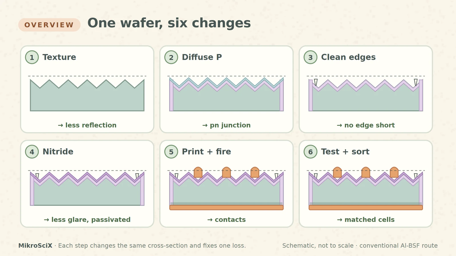
A freshly sawn silicon wafer reflects about a third of the light that hits it and cannot deliver any current. Six factory steps change that: texture, emitter diffusion, cleaning and edge isolation, a nitride coating, printed and fired contacts, and a light test. This guide follows one cross-section through the conventional aluminium back-surface-field (Al-BSF) route and asks, for each step, which loss it removes. For undergraduate and graduate students.
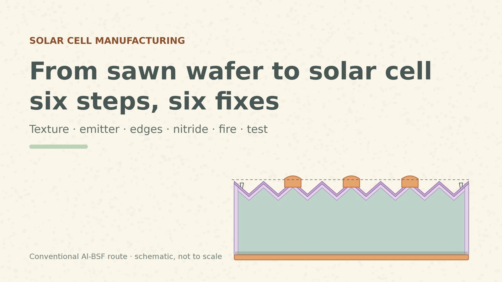
Start with a p-type monocrystalline wafer, about 180 µm thick, cut from an ingot with a diamond-coated wire saw [S1][S2]. It is grey, flat and electrically boring: no junction, no contacts, a shiny surface that throws light back, and a skin damaged by the saw. A working cell needs every one of those fixed. The sequence below is the one a 2015 dissertation on industrial Al-BSF cells lists step by step: saw damage removal and texturing, phosphorus diffusion, glass removal and edge isolation, silicon nitride, screen printing, co-firing, then light I–V testing and sorting [S2].
Each section gives the rule, a number you can check yourself, and what breaks. The drawings are schematic: a real pyramid is a few micrometres, the emitter at most about two, the nitride 70 nanometres, and the wafer about 180 micrometres.
1. Texture: carve pyramids into the surface
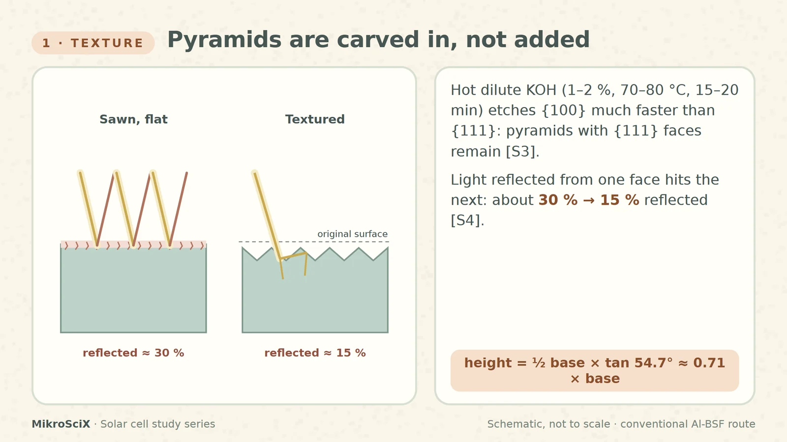
The first wet step does two jobs. A strong alkaline etch removes the layer the saw damaged, and a hot, dilute one textures what is left [S1][S3]. One typical recipe is 1–2 % KOH at 70–80 °C for 15–20 minutes. The trick is crystallography: the alkaline solution attacks the {100} surface of the wafer much faster than the {111} planes, so the etch stops on {111} facets and leaves random pyramids. Their ideal face angle is 54.74°, and pyramids with a 3–10 µm base work best [S3].
Why bother? Bare silicon reflects roughly 30 % of the incident light. On pyramids, a ray reflected from one face usually hits a neighbouring face and gets a second chance to enter, and reflection falls to around 15 % [S4].
Check it yourself. Of 100 photons, a flat wafer lets 70 in and a textured one 85. That is 85 / 70 ≈ 1.21: about 21 % more light inside before any coating. And a pyramid with a 5 µm base is 2.5 µm × tan 54.7° ≈ 3.5 µm tall, about 2 % of the wafer thickness.
What breaks. Pyramids are etched into the wafer: the tips end at or below the original surface, nothing is added on top. Uneven texture makes printed fingers spread wider and shade more [S2]. Multicrystalline wafers do not texture well in alkali and need other methods [S10].
2. Phosphorus diffusion: build the junction inside the silicon
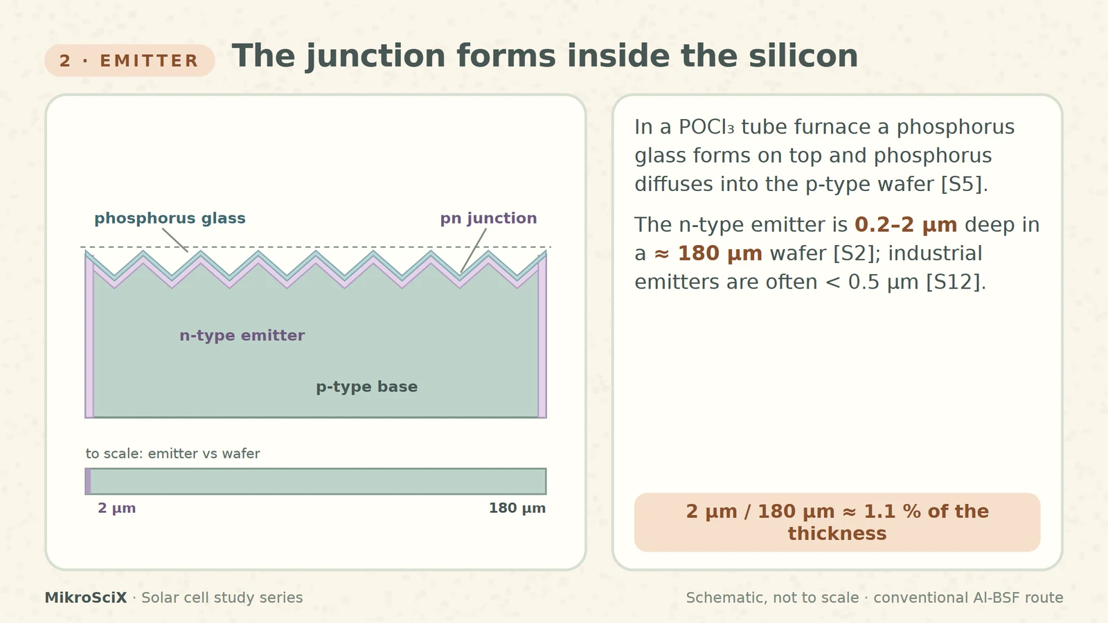
A p-type wafer needs an n-type region to form a pn junction. In a quartz tube furnace, nitrogen carries vapour from liquid POCl₃ over the wafers; a phosphosilicate glass (PSG) forms on the surface, and phosphorus is driven from it into the silicon [S5]. The top of the wafer becomes the n-type emitter; below it the p-type base continues. The junction sits where they meet, inside the crystal.
Check it yourself. The dissertation gives an emitter 0.2–2 µm deep on a substrate of about 180 µm [S2]. Even the deep end is 2 / 180 ≈ 1.1 % of the thickness; industrial POCl₃ emitters are often thinner than 0.5 µm [S12].
What breaks. The emitter is not a layer painted on top; the glass is. And more phosphorus is not simply better: heavily doped near-surface layers raise the emitter saturation current and cut the blue response, which is why lighter emitters are studied [S12]. The contacts, on the other hand, need a high phosphorus concentration right under them [S10].
3. Clean up: strip the glass, cut the edges
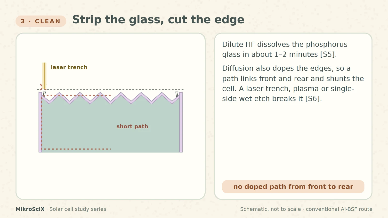
The PSG has done its job and comes off in a short dip in dilute hydrofluoric acid, about 1–2 minutes, followed by a rinse [S5]. A second problem is less visible. During diffusion the whole wafer surface is exposed, edges included, so a continuous doped path runs from the front emitter round the edge to the rear. That path shunts the finished cell: carriers that take it never reach the load [S6].
Edge isolation breaks it. Production lines use a CF₄/O₂ plasma on stacked wafers, a single-side wet etch in HF/HNO₃, or a laser trench through the front surface close to the edge [S6].
Check it yourself. Trace the lilac region in the figure: before the cut you can walk from the front emitter to the rear without leaving doped silicon; after it you cannot.
What breaks. Too short a plasma step leaves the path; too long damages the edges and adds recombination. Wet etchant splashing onto the front attacks the emitter [S6].
4. Silicon nitride: one film, two jobs
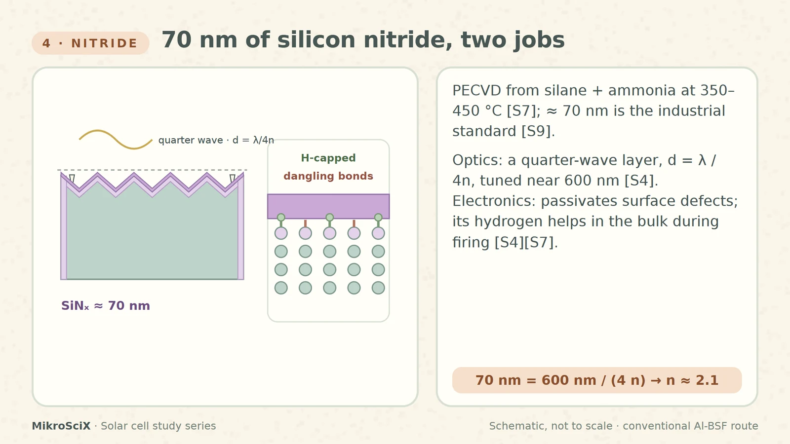
Next comes a thin silicon nitride (SiNₓ:H) layer, grown by plasma-enhanced CVD from silane and ammonia on a wafer heated to about 350–450 °C [S7]. About 70 nm is the industrial standard for front passivation and antireflection [S9]. It sits on the silicon, following the pyramids.
Optically it is a quarter-wave layer: its thickness is chosen so that d = λ / 4n near 600 nm, close to the peak of sunlight, and it lowers reflection beyond what the pyramids achieve [S4]. Electronically it passivates the surface, where broken bonds would otherwise let electrons and holes recombine, and its hydrogen moves into the silicon during firing and passivates defects there too [S4][S7]. The dissertation adds that the same layer serves as the front passivation of the Al-BSF cell [S2].
Check it yourself. If a 70 nm film is a quarter wave at 600 nm, then n = 600 / (4 × 70) ≈ 2.1. A film of n = 2.0 would need 600 / 8 = 75 nm.
What breaks. The nitride is an insulator. Metal printed on it does not touch the silicon until firing opens a path, and the deposition conditions change how easily the paste can get through [S8].
5. Print and fire: contacts through the nitride
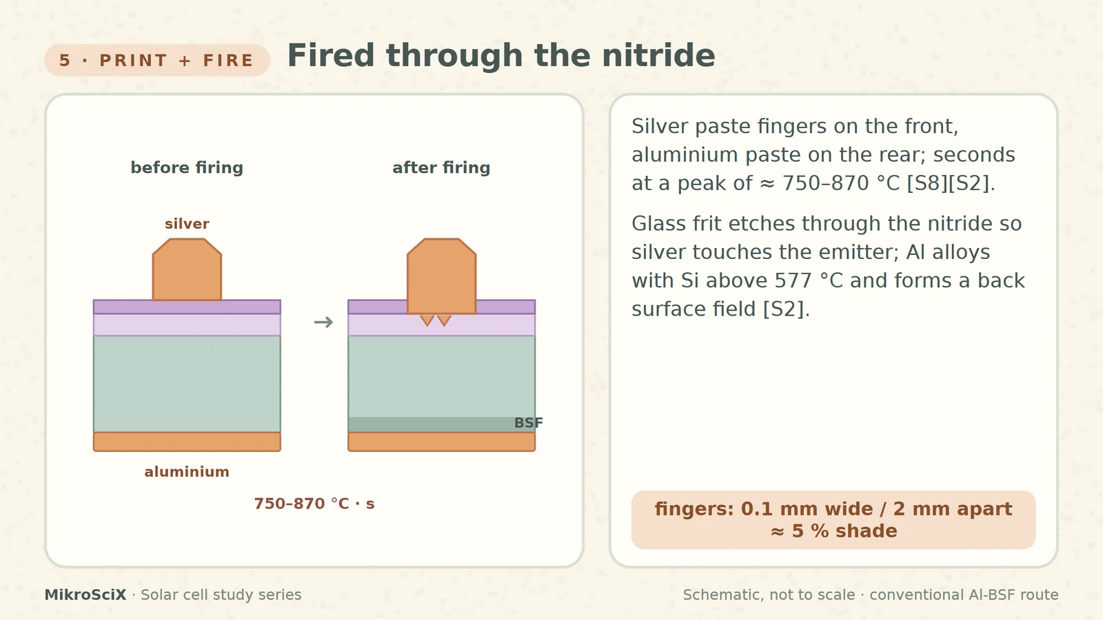
Silver paste is screen-printed as narrow fingers and busbars on the front; aluminium paste covers the rear [S2][S10]. The pastes are dried and then co-fired in an in-line infrared furnace: a few seconds at a peak of roughly 750–870 °C [S8]. The dissertation describes the same profile with 750–800 °C and a 1–3 s dwell [S2].
Two things happen in those seconds. On the front, the glass frit in the silver paste etches through the nitride, so silver crystallites grow on the emitter and make an ohmic contact. On the rear, aluminium starts alloying with silicon above the Al–Si eutectic temperature of 577 °C; on cooling, aluminium-doped silicon recrystallises and forms a p⁺ back surface field (BSF), which reduces recombination at the rear [S2].
Check it yourself. Fingers 100 µm wide every 2 mm cover 0.1 / 2 = 5 % of the front. With busbars, the dissertation gives about 5–8 % shading for 70–120 µm gridlines [S2].
What breaks. Under-fired, the frit does not open the nitride and contact resistance stays high; over-fired, a thick glass layer and overgrown silver crystallites lower the shunt resistance [S2].
6. Test and sort
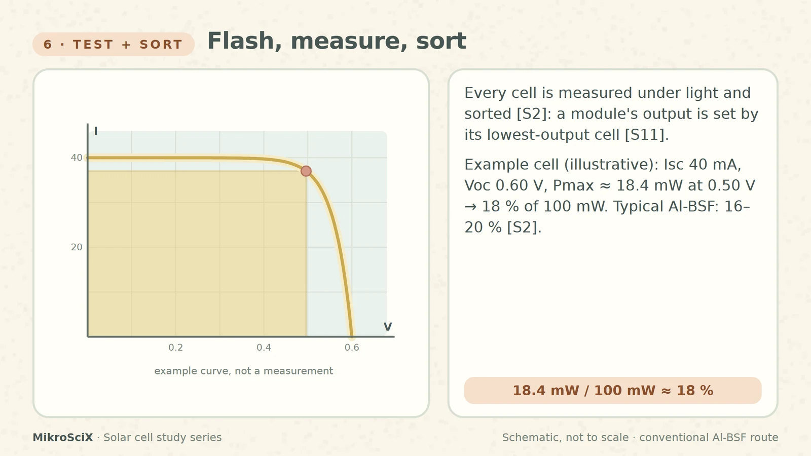
Every finished cell is flashed and its light I–V curve recorded, then it is sorted [S2]. Sorting matters because cells are later connected into modules, and the output of a whole module is set by its lowest-output cell [S11]. Stringing and lamination are a separate story; this is where the cell ends.
Check it yourself. Take the series' example cell, an ideal diode with Isc = 40 mA and Voc = 0.60 V on 1 cm². Its maximum power is about 18.4 mW near 0.50 V; under 100 mW of light that is about 18 %. Real industrial Al-BSF cells sit at about 16–20 % [S2]. The example is a teaching curve, not a measurement.
What newer cells change
Everything here is the conventional full-aluminium BSF route. PERC cells differ mainly at the rear: the rear is passivated and contacted only locally through openings [S2]. Other architectures change more. The logic stays the same: each layer is there to remove one loss.
Texture lets light in, phosphorus builds the junction inside the silicon, clean edges stop the short, nitride cuts glare and heals the surface, and firing pushes the metal through to the silicon.
Try it yourself
- A pyramid has an 8 µm base. How tall is it? 4 µm × tan 54.7° ≈ 5.7 µm.
- Fingers 80 µm wide every 1.6 mm. What fraction do they shade (busbars ignored)? 0.08 / 1.6 = 5 %.
- A nitride with n = 2.0 should be a quarter wave at 600 nm. How thick? 600 / (4 × 2.0) = 75 nm.
- The example cell at 0.45 V gives 39.1 mA. What power? 0.45 V × 39.1 mA ≈ 17.6 mW, a little below the 18.4 mW maximum.
Watch the short
Videos don’t load automatically. The videos are hosted on YouTube. Allow YouTube once and every video on the site loads by itself; your choice is remembered. The articles never need consent.
Sources
- U.S. Department of Energy — Solar Photovoltaic Manufacturing Basics
- N. Chen — Understanding and development of cost-effective industrial Al-BSF silicon solar cells (PhD dissertation, UNC Charlotte, 2015)
- PV Manufacturing (UNSW / ASU) — Alkaline texturing
- PV Manufacturing — Antireflection coating
- PV Manufacturing — Tube diffusion
- PV Manufacturing — Edge isolation
- PV Manufacturing — PECVD of silicon nitride
- PV Manufacturing — PVFactory 8: Cofiring
- Schwab, Hofmann, Rentsch, Preu (Fraunhofer ISE) — Front surface passivation by silicon oxynitride–silicon nitride stacks, 25th EU PVSEC 2010
- PVEducation — Screen Printed Solar Cells
- PVEducation — Mismatch Effects
- Komatsu et al. — The potential advantage of industrially processed boron emitters compared to phosphorus emitters, Energy Procedia 55 (2014)
- Penn State EME 812 — Lesson 4: Photovoltaics
Diagrams are schematic and not to scale. Conventional p-type Al-BSF route; PERC and other architectures differ. The I–V curve is the series' ideal-diode example (Isc 40 mA, Voc 0.60 V, 1 cm²), not a measurement.